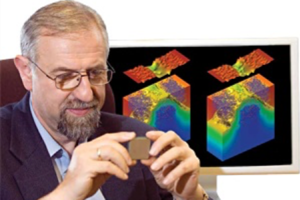
 Semiwise in Glasgow has developed transistor SPICE models for cryogenic CMOS chip design and verification using the GlobalFoundries (GF) 22FDX 22nm fully depleted silicon-on-insulator (FD-SOI) process technology. The technology can be used for chips for quantum computers and also for data center processors with liquid nitrogen cooling.
Semiwise used its patented ‘re-centering’ technology to develop models for typical (TT) fast (FF) and slow (SS) transistor corners. This includes combination transistor measurements and TCAD simulations using the cryogenic-proven Synopsys Sentaurus device simulator. The ‘re-centering’ process is automated using the Synopsys TCAD-to-SPICE flow, which is part of the Synopsys Design Technology Co-Optimization (DTCO) tool chain.
Semiwise develops low-power CMOS transistor-level IP that improves performance and variability, and drastically reduces power consumption as well as simulation services and consulting to the semiconductor industry including fables, IEDM and foundry players.
The CEO of Semiwise, Professor Asen Asenov, was the founder of Gold Standard Simulations (GSS), a 2010 startup from the University of Glasgow which developed the first TCAD based Design-Technology Co Optimization (DTCO) tool chain. After the acquisition of GSS by Synopsys in 2016 the TCAD-to-Spice technology originally developed by GSS is now part of the Synopsys TCAD offering in the TCAD-to-Spice flow.
Design of cryogenic CMOS chips is vital for the scaling of different types of quantum computers to accommodate the large number of quantum bits (q-bits) needed for solving real-life problems. The current bottleneck is related to the very low temperature (anywhere from 77K to a fraction of a Kelvin) of operation of the q-bits housed in cryostats.
Many cables take information from the q-bits to room-temperature CMOS chips outside of the cryostat that read, condition and process the ‘quantum’ information. As a result, only relatively small numbers of q-bits can be housed in a single large cryostat.
This temperature reduction results in drastic changes of the transistor characteristic, rendering room-temperature chip design and the corresponding chip technologies unsuitable for cryogenic chip operation. Most of the current technologies require significant re-optimization to enable cryogenic chip operation.
However, in the GF 22FDX Platform, the transistor parameters can be flexibly altered by electrical (back) biasing to compensate for the low temperature changes. This makes the technology directly applicable to cryogenic chip design as it stands.
Semiwise has also developed a tool called ‘Recenter’ that allows the models can be seamlessly included in the standard EDA tool flow based on the GF 22FDX Platform Process Design Kit (PDK).
The models can also be used to design COLD CMOS chips for data centers that can operate at liquid nitrogen temperatures. A recent study from Synopsys shows that if processors and other chips are operated at 77K, the power dissipation can be reduced ~7x at equivalent speed.
“The cryogenic chip design will not only unleash the true power of quantum computers but will increase significantly the energy efficiency of the data centers in the transition to a net zero economy,” said Professor Asen Asenov, CEO of Semiwise.
www.semiconductorwise.com; www.synopsys.com/silicon/tcad.html
Image courtesy of: eeNews Europe
Source: eeNews Europe


